Q1. With a neat circuit diagram and waveforms explain the operation of Master Slave JK flip flop
geeksforgeeks.org/master-slave-jk-flip-flop/ The Master-Slave JK flip-flop is designed to overcome the race around condition encountered in basic JK flip-flops when both inputs J=1J = 1 and K=1K = 1 with a prolonged clock pulse. In such cases, the output toggles continuously and unpredictably while the clock is high, causing unstable output.
Circuit Diagram:
Below is the simplified logic diagram of a Master-Slave JK Flip-Flop:

Working Principle:
-
Master-Slave JK flip-flop consists of two JK flip-flops connected in series:
-
The Master is positive level triggered (active when clock = 1)
-
The Slave is negative level triggered (active when clock = 0)
-
-
The clock signal is inverted and fed into the Slave, meaning it operates on the opposite phase of the Master.
Operation Based on Inputs:
| J | K | Operation |
|---|---|---|
| 0 | 0 | No Change (Q remains the same) |
| 0 | 1 | Reset (Q → 0) |
| 1 | 0 | Set (Q → 1) |
| 1 | 1 | Toggle (Q → Q’) |
Step-by-Step Explanation:
- Clock HIGH (CP = 1):
- Master is enabled, Slave is disabled.
- Inputs J and K affect the Master.
- Output Qm of Master is updated based on JK logic.
- Slave holds its previous state.
- Clock LOW (CP = 0):
- Master is disabled, Slave is enabled.
- Slave takes input from Master’s output (Qm).
- The final output Q is updated.
Case Analysis:
- J = 0, K = 0: No change. Output remains as is.
- J = 0, K = 1: Master resets → Slave resets → Q = 0.
- J = 1, K = 0: Master sets → Slave sets → Q = 1.
- J = 1, K = 1: Master toggles → Slave toggles → Q toggles once per clock cycle (no race).
Timing Diagram:
- The master changes state on the rising edge of CLK.
- The slave changes on the falling edge, copying the master’s output.
- This ensures only one toggle per clock cycle, removing the race condition.
Q2. Design a MOD5 synchronous counter using JK flip-flop?
https://www.slideshare.net/slideshow/mod5synchronouscounterusingjk-flipfloppdf/265448520


Q3. Design a 4 bit universal shift resister and draw the circuit with the given mode of operation table.
https://www.youtube.com/watch?v=otUEfWgUSkQ
Q4. Write a short note on followings:
a) CMOS transmission gate
b) Tristate TTL
c) AND, OR gates using DTL.
https://buzztech.in/cmos-transmission-gate/ https://www.eeeguide.com/what-is-tristate-logic-or-three-state-logic-circuit/ https://www.elprocus.com/diode-transistor-logic/
a) CMOS Transmission Gate (Pass Gates)
A CMOS Transmission Gate (TG) consists of one nMOS and one pMOS transistor connected in parallel. The control signals applied to their gates are complementary, allowing the gate to function as a bidirectional switch between two nodes.
-
When the control signal is high, both transistors turn on, creating a low-resistance path.
-
When the control signal is low, both transistors turn off, resulting in a high-impedance (open circuit) state.

-
NMOS passes good 0s but poor 1s; PMOS passes good 1s but poor 0s.
-
Together, they compensate each other, enabling full voltage swing.
-
Used in implementing multiplexers, XOR/XNOR gates, latches, and flip-flops.
-
Offers low output degradation and low propagation delay.
-
Requires both true and complement control signals.
-
Increases node capacitance due to parallel transistor connections.
Dynamic Analysis: Can be modeled as a simple resistor for transient analysis when ON.
b) Tristate TTL (Three-State Logic)
Tristate logic introduces a third output state — High Impedance (Hi-Z) — in addition to the usual HIGH and LOW states.
- In Hi-Z state, the output is effectively disconnected from the circuit, behaving like an open circuit.
- Allows multiple outputs to be connected to a common bus without interference, provided only one is enabled at a time.


 Operation:
 - Controlled by an ENABLE input:
- If ENABLE = 1 → normal operation (output active).
- If ENABLE = 0 → output enters Hi-Z state.
Applications:
- Widely used in microprocessors, memory systems, and data buses.
- Enables bus-oriented communication where multiple devices share a single line.
Advantages:
- High-speed operation similar to totem-pole outputs.
- Facilitates wired-AND configurations without external diodes or resistors.
- Prevents short circuits and excessive current draw.
Disadvantage:
- Only one device should be enabled on the bus at a time to avoid conflicts.
c) AND, OR Gates Using DTL (Diode-Transistor Logic)
DTL is an early digital logic family that uses diodes for logic functions and transistors for amplification/output driving.
DTL AND Gate:

- Constructed using a diode AND configuration followed by a transistor inverter.
- Diodes are connected in series with their cathodes tied together and connected to the base of the transistor through a resistor.
- If all inputs are HIGH, the transistor turns ON, pulling output LOW (logical 0).
- If any input is LOW, the transistor remains OFF, and output is HIGH (logical 1).
DTL OR Gate:
- Uses a diode OR configuration followed by a transistor stage.
- Diodes are connected in parallel with anodes receiving input signals.
- If any input is HIGH, the transistor turns ON, pulling output LOW.
- If all inputs are LOW, the transistor remains OFF, and output is HIGH.
Q5. Draw a totem-pole output buffer with a TTL gate. Explain its operation
Q5. Draw a Totem-Pole Output Buffer with a TTL Gate and Explain its Operation
The diagram below represents a TTL (Transistor-Transistor Logic) NAND gate with a totem-pole output configuration, commonly used in digital circuits:
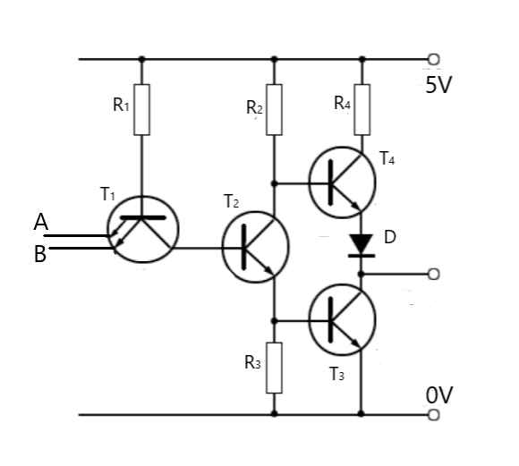
This circuit includes the following components:
- T₁: Input transistor with two emitters (for receiving multiple inputs).
- T₂, T₃: Intermediate transistors for amplification and signal processing.
- T₄ and T₅: Output transistors arranged in a totem-pole configuration (one above the other).
- D: Diode to prevent both output transistors from being ON simultaneously.
- Resistors (R₁, R₂, R₃) for biasing and current control.
Operation of the Totem-Pole Output Buffer in TTL NAND Gate
Case: Inputs A = 1, B = 1 (Both HIGH)
- The base-emitter junction of T₁ is reverse-biased → T₁ is OFF.
- The collector voltage of T₁ rises to ~5V.
- This voltage drives the base of T₂, turning it ON.
- As T₂ conducts, its collector voltage drops, turning T₃ ON (saturated).
- Collector voltage of T₃ ≈ 0.2V (LOW output).
- The base voltage of T₄ is derived from T₃’s base-emitter and collector-emitter voltages (~0.9V).
- The emitter of T₄ is at T₃’s collector voltage + diode drop (~0.7V) = 0.9V.
- Since base voltage ≈ emitter voltage, T₄ is OFF.
- T₅ is ON due to base drive through R₃.
- Output Y ≈ 0.2V (Logic LOW).
Case: Any Input LOW (A = 0 or B = 0)
- The base-emitter junction of T₁ is forward-biased → T₁ is ON.
- Collector voltage of T₁ drops → T₂ is OFF.
- Base of T₃ receives no drive → T₃ is OFF.
- Base of T₄ is pulled high through R₂ → T₄ is ON.
- T₅ is OFF since its base has no drive.
- Output is pulled up to VCC through T₄.
- Output Y ≈ 5V (Logic HIGH).
Truth Table for TTL NAND Gate with Totem-Pole Output
| A | B | Y (Output) |
|---|---|---|
| 0 | 0 | 1 |
| 0 | 1 | 1 |
| 1 | 0 | 1 |
| 1 | 1 | 0 |
In TTL logic, the totem-pole output refers to the arrangement of two transistors (T₄ and T₅ in this case) stacked vertically between VCC and GND. Only one transistor is ON at any time:
- T₄ (Upper transistor) pulls the output HIGH.
- T₅ (Lower transistor) pulls the output LOW.
The diode D ensures that both transistors do not conduct simultaneously, avoiding short-circuit conditions.
Q6. Explain MOS& CMOS open drain and tristate outputs?
MOS and CMOS Open Drain and Tristate Outputs Explained
In digital electronics, especially in MOS (Metal-Oxide-Semiconductor) and CMOS (Complementary MOS) logic families, the output configurations of gates can vary to suit different applications. Two important types are:
- Open Drain Output
- Tristate Output
Let’s explore each in detail.
1. Open Drain Output (MOS / CMOS)
What is an Open Drain Output?
An open drain output is a type of configuration used in MOS logic circuits, particularly in CMOS technology, where the output transistor is an n-channel MOSFET with its drain left open (not connected internally to VDD).
- The source is connected to ground.
- The gate receives the internal signal.
- An external pull-up resistor is required to connect the drain to VDD to produce a HIGH output.

Circuit Configuration:
- Only an nMOS transistor is used at the output stage.
- No pMOS transistor for active pull-up.
Operation:
- When the nMOS is ON, it pulls the output LOW (connected to GND).
- When the nMOS is OFF, the output is HIGH impedance, and the external pull-up resistor pulls the output to HIGH.
Truth Table Example:
| Input | Output Transistor | Output |
|---|---|---|
| 0 | OFF | HIGH (via pull-up) |
| 1 | ON | LOW |
Applications:
- Wired-AND logic: Multiple open-drain outputs can be tied together with a single pull-up resistor.
- I²C communication: Used in I²C bus systems where multiple devices share the same line.
- Voltage translation: Allows interfacing between different voltage domains.
Advantages:
- Allows multiple devices to share a common line.
- Can drive loads requiring higher current (with proper pull-up).
- Supports voltage level shifting.
Disadvantages:
- Requires external pull-up resistor.
- Slower rise time due to RC charging from the pull-up resistor and load capacitance.
2. Tristate Output (CMOS)
What is a Tristate Output?
A tristate output has three possible states:
- Logic HIGH
- Logic LOW
- High Impedance (Hi-Z) — effectively disconnects the output from the circuit.
This allows multiple outputs to be connected to a common bus, provided only one is enabled at a time.
Circuit Configuration:
- Uses both pMOS and nMOS transistors in a standard CMOS push-pull configuration.
- Includes enable/disable control inputs that turn off both transistors simultaneously to enter Hi-Z state.

Applications:
- Bus architectures in microprocessors and memory systems.
- Data multiplexing where multiple sources share a single data path.
- Prevents bus contention by ensuring only one device drives the bus at a time.
Advantages:
- Enables shared bus communication.
- High-speed operation when active.
- Low power consumption in Hi-Z mode.
Disadvantages:
- Requires control logic to manage enable signals.
- Risk of bus conflict if more than one device is enabled at the same time.
Q7. Draw the circuit diagram of Inverting. Non-Inverting operational amplifier and explain its working.
https://www.electronics-tutorials.ws/opamp/opamp_2.html
Inverting and Non-Inverting Operational Amplifier Circuits – Diagrams & Working
Operational amplifiers (op-amps) are widely used in analog electronics for signal conditioning, filtering, and amplification. Two of the most common configurations are:
- Inverting Operational Amplifier
- Non-Inverting Operational Amplifier
Let’s explore both with circuit diagrams, their working principles, and key formulas.
Inverting Operational Amplifier
Circuit Diagram:

- Vin: Input voltage applied through resistor Rin
- Rf: Feedback resistor from output to inverting input
- (-): Inverting terminal
- **(+)]: Non-inverting terminal grounded
Working Principle:
- The non-inverting input is connected to ground (0V).
- The inverting input becomes a virtual ground due to negative feedback — meaning it’s at the same potential as the non-inverting input but no current flows into the op-amp.
- A feedback resistor (Rf) connects the output back to the inverting input, creating a closed-loop gain.
- The input resistor (Rin) separates the input signal from the virtual ground point.
Key Equations:
- Voltage Gain (Av):
- Output Voltage (Vout):
The negative sign indicates that the output is 180° out of phase with the input — hence, it’s called an inverting amplifier.
Characteristics:
| Feature | Description |
|---|---|
| Phase Shift | 180° |
| Input Impedance | Equal to Rin |
| Output Polarity | Opposite of input |
| Use Case | Signal inversion, transimpedance amp |
Applications:
- Signal inversion
- Transimpedance (current-to-voltage conversion)
- Audio mixers
- Sensor signal amplification
Non-Inverting Operational Amplifier
Circuit Diagram:

- Vin: Applied directly to the non-inverting input (+)
- Feedback network: Resistor divider formed by Rf and Rin
- Inverting input (-) receives feedback from output via Rf and Rin
Working Principle:
- The input signal is applied to the non-inverting terminal (+).
- A voltage divider formed by Rf and Rin provides negative feedback to the inverting terminal.
- Due to negative feedback, the differential input voltage is nearly zero, i.e., V+ ≈ V−.
- This configuration does not invert the signal — output is in phase with the input.
Key Equations:
- Voltage Gain (Av):
- Output Voltage (Vout):
There is no negative sign, so the output is in-phase with the input.
Characteristics:
| Feature | Description |
|---|---|
| Phase Shift | 0° |
| Input Impedance | Very high (ideally infinite) |
| Output Polarity | Same as input |
| Use Case | Voltage follower, buffer, gain stages |
Applications:
- Buffer amplifier
- Voltage follower
- High-impedance sensor interface
- Audio preamplifiers
Q8. Write all the DC and AC characteristics of an ideal OP-AMP with relevant expressions
DC Characteristics
| Characteristic | Description | Value for Ideal Op-Amp |
|---|---|---|
| Input Impedance | Resistance seen at the input terminals | Infinite (∞) |
| Output Impedance | Resistance seen at the output terminal | Zero (0) |
| Common-Mode Rejection Ratio (CMRR) | Ability to reject signals common to both inputs | Infinite (∞) or Acm = 0 |
| Open-Loop Gain (Ad) | Voltage gain without feedback | Infinite (∞) |
| Offset Voltage | Voltage required at input to make output zero | Zero (0) |
| Bias Current | Current drawn by the input terminals | Zero (0) |
| Offset Current | Difference between the two input bias currents | Zero (0) |
AC Characteristics
| Characteristic | Description | Value for Ideal Op-Amp |
|---|---|---|
| Bandwidth | Range of frequencies over which the op-amp operates effectively | Infinite (∞) |
| Slew Rate (SR) | Maximum rate of change of output voltage per unit time | Infinite (∞) |
| Rise Time | Time taken for the output to rise from 10% to 90% of its final value | Zero (0) |
| Settling Time | Time taken for the output to settle within a specified error band | Zero (0) |
| Phase Shift | Change in phase between input and output | Zero (0°) across all frequencies |
Difference Amplifier
The difference amplifier amplifies the difference between two input voltages and suppresses the common-mode signal.
🔹 Input Signals
Where:
- : Differential input voltage
- : Common-mode input voltage
🔹 Output Voltage
Where:
- : Differential gain
- : Common-mode gain
🔹 CMRR (Common-Mode Rejection Ratio)
For an ideal op-amp, , so CMRR → ∞.
Q9. Derive closed loop voltage gain, input resistance, output resistance and band width for inverting amplifier with feedback arrangement.
https://circuitdigest.com/tutorial/inverting-operational-amplifier-op-amp
1. Closed-Loop Voltage Gain ()
The closed-loop voltage gain is determined by the ratio of the feedback resistor () to the input resistor ():
The negative sign indicates a 180° phase shift between input and output.
2. Input Resistance ()
The input resistance is equal to the input resistor:
This is because the inverting input is at virtual ground, and the op-amp’s input draws negligible current.
3. Output Resistance ()
Negative feedback reduces the output resistance of the amplifier. The closed-loop output resistance is given by:
Where:
-
is the open-loop output resistance of the op-amp.
-
is the open-loop voltage gain of the op-amp.
-
is the feedback factor, given by:
Since is typically very large, the term is also large, making very small.
4. Bandwidth (BW)
The gain-bandwidth product (GBW) of an op-amp is constant:
Therefore, the bandwidth of the inverting amplifier is:
This implies that as the closed-loop gain increases, the bandwidth decreases proportionally, maintaining a constant GBW.